AU sensor chips
XanTec’s AU sensor chips consist of an approximately 44 nm gold layer deposited on a borosilicate glass substrate. These chips are intended for custom surface development or use as a reference surface.
Direct adsorption-based ligand immobilization is generally not recommended, as it frequently results in partial ligand denaturation and elevated nonspecific background signals, limiting suitability for standard SPR interaction analyses.
Key features:
- Base sensor chip: Provides a clean, well-defined gold surface suitable for development and evaluation of custom surface chemistries.
- Surface conductive for Electro-SPR (E-SPR): Enables electrochemical SPR applications.
- Reference chip: Serves as a control surface for assessing nonspecific interactions or benchmarking newly developed coatings.
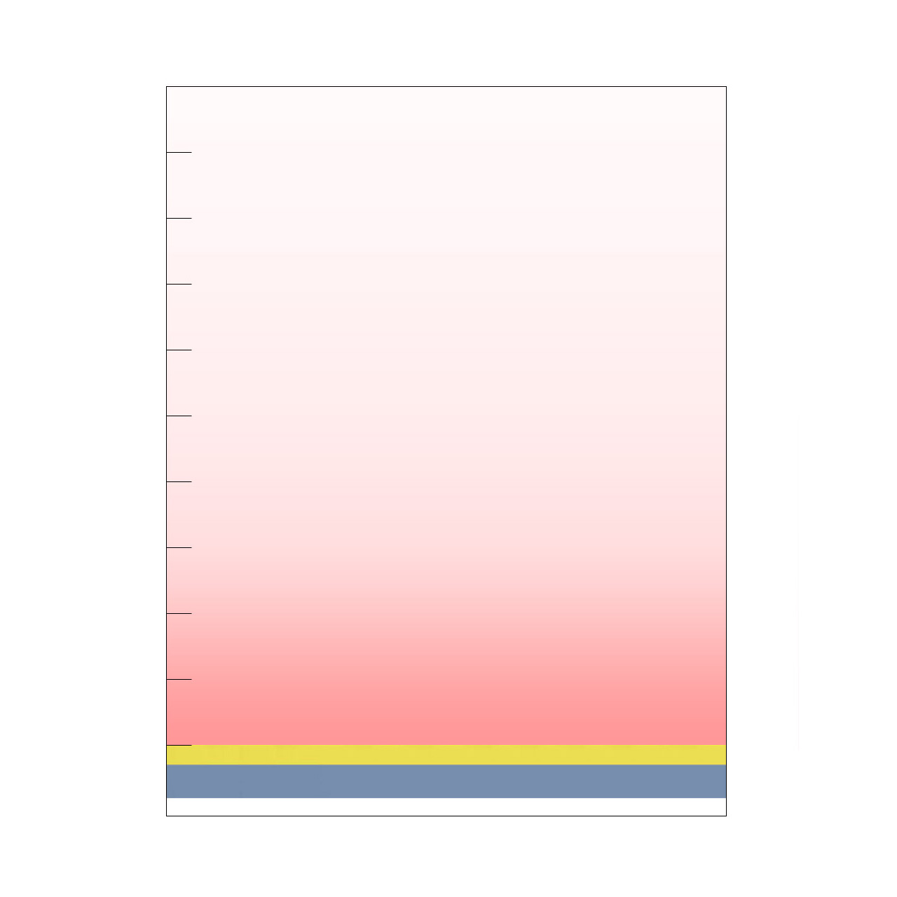
Schematic illustration of a bare AU sensor chip. The decaying red gradient represents the evanescent field.1
| Product code | Au |
|---|---|
| Base coating | Bare gold, ≈ 44 nm, on borosilicate glass support |
| Intended purpose |
|
1 All illustrations are schematic representations and are not drawn to scale; dimensions, densities, and spatial relationships do not reflect actual physical or chemical proportions.